"Successful engineering is all about understanding how things break or fail."
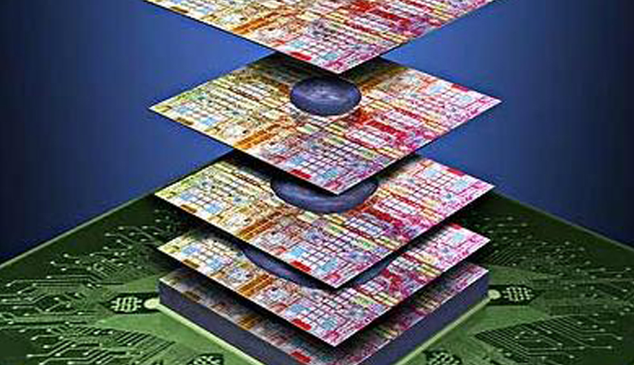
After receiving his bachelor and Master’s degrees from France in the same year, Engineer Elie Eid, PhD, quickly got into academia started teaching many courses, in parallel with working on his doctoral thesis entitled: "Characterization and modelling of the coupling effects by the substrates in the stacking up of the 3D integrated circuits".
The purpose of his research was to quantify and predict the substrate coupling phenomena that can occur in 3D integrated circuits. In order to improve the electrical performance in such cases; a large electromagnetic modeling and a high frequency characterization are required.
"Through Silicon Vias" or TSV are numerous vertical coupling interconnections existing in a small volume and passing through silicon. In order to minimize the coupling effects in RF substrates; Dr. Eid proposed rules for electrical performance optimization. For that matter; different test structures configurations were used to analyze the coupling. The characterizations are performed on a very wide frequency spectrum.
The analysis held these following parameters:
- Thickness of the substrate
- TSV architectures (diameters, densities, types of barriers)
- Nature of the used materials.
A considerable amount of 3D modeling was conducted through this research to compare measurements with simulations and validate results. Optimization strategies to reduce coupling phenomena in 3D circuits have been proposed; this has provided a wealth of information to designers.